Modern SD cards, MicroSD cards, and many USB flash drives use monolithic construction: the NAND memory and controller are sealed together in a single epoxy package with no separately accessible NAND chip. When the controller portion fails, no card reader or software tool can detect the device. The only path to the data is direct NAND extraction through the chip's internal test points.
This page documents the monolithic chip families we encounter most frequently, the signal interfaces used in direct NAND access, and the spider board technique that makes extraction possible without soldering wires onto microscopic pads.
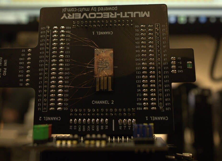
Spider board adapter with needle probes contacting exposed NAND test points on a monolithic microSD card. Each needle maps to a specific flash signal line.

In a traditional SD card or USB drive, the NAND flash memory and the controller are separate components on a small PCB. If the controller fails, a technician can desolder the NAND chip and read it directly in a programmer. The chip has standardized pins (TSOP48 or BGA) that connect to off-the-shelf adapters.
Monolithic designs eliminate the PCB entirely. The controller logic and NAND memory are sealed together in one plastic or epoxy package with only the external contact pads exposed. There is no NAND chip to desolder because the dies are wire-bonded inside a single package rather than mounted as a separate, removable chip.
When a monolithic controller fails, the external contacts go completely dead. The device does not appear in Disk Management, does not show in lsblk, and cannot be detected by any software. The NAND memory cells still hold your data, but the only way to reach them is through test points on the silicon die that sit beneath a layer of protective epoxy.
Accessing those test points requires sanding away the epoxy with a fiberglass pen, identifying each pad's signal assignment from a pinout database, and making electrical contact with each one simultaneously. This is why monolith recovery is the most labor-intensive form of flash data recovery.
Every monolithic flash chip routes the standard NAND interface signals to internal test points. The spider board must make contact with each of these signals to read the raw memory. Missing or misidentified signals produce a corrupt dump or no data at all.
| Signal | Full Name | Direction | Function |
|---|---|---|---|
| D0-D7 | Data Bus | Bidirectional | 8-bit parallel data transfer between host and NAND. All read/write data passes through these lines. |
| CE# | Chip Enable | Input | Active-low. Selects the NAND die for communication. Multi-die packages may have CE0# and CE1#. |
| CLE | Command Latch Enable | Input | When high, tells the NAND that the data bus carries a command byte (read, write, erase, status check). |
| ALE | Address Latch Enable | Input | When high, tells the NAND that the data bus carries an address byte (which page/block to access). |
| WE# | Write Enable | Input | Active-low. Latches data, commands, or addresses from the data bus on the rising edge. |
| RE# | Read Enable | Input | Active-low. Clocks data out of the NAND onto the data bus during read operations. |
| WP# | Write Protect | Input | Active-low. Prevents write and erase operations. Must be held high during recovery reads. |
| R/B# | Ready/Busy | Output | Open-drain output. Low when the NAND is busy (internal read/write/erase in progress). High when ready for next command. |
| VCC | Power Supply | Power | 3.3V for most SD/MicroSD NAND. Some newer dies use 1.8V I/O with 3.3V core. Incorrect voltage damages the die. |
| VSS | Ground | Power | Ground reference. Multiple VSS pads often exist on the die. All must be connected for stable signal integrity. |
ONFI vs Toggle: Micron and Intel/SK Hynix NAND use the ONFI (Open NAND Flash Interface) protocol. Samsung, SanDisk/WD, and Kioxia (formerly Toshiba) NAND use the Toggle-mode interface. Both protocols use the same signal names but differ in timing and data latching behavior. PC-3000 Flash supports both protocols but requires selecting the correct mode before attempting a read.
The spider board is a PC-3000 Flash adapter that holds adjustable needle probes on micro-positioners. Each needle makes contact with one test point on the exposed NAND die. The technician aligns each needle by hand under a microscope, matching probe positions to signal assignments from the PC-3000 pinout database.
The process demonstrated in our filmed spider board recovery shows the full procedure: scraping the epoxy with a fiberglass pen, identifying pad locations against the database, and placing each needle onto its assigned signal. Chris, our flash recovery technician, placed 17 individual needles on a single microSD card in that session.
The older method: solder 30 AWG (or finer) jumper wires directly onto each test point, then connect each wire to the corresponding pin on a PC-3000 Flash circuit board adapter. This was the standard approach before spider boards existed and is still used when test points are too deeply recessed for needle contact.
Wire soldering requires a micro-tipped iron, flux, and magnification. Each solder joint must bridge a pad that may be smaller than 0.1 mm across. A solder bridge between adjacent pads creates a short that can corrupt the read or damage the die. Flux residue can also cause intermittent signal issues if not cleaned.
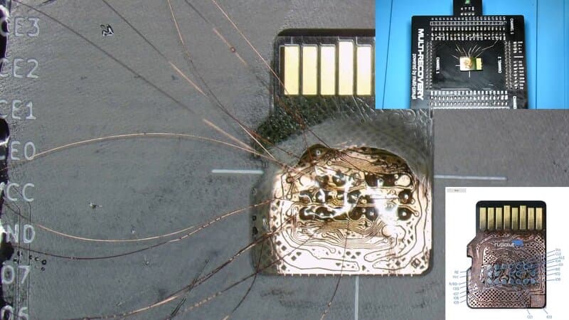
Spider board wiring from our lab: each needle contacts a single test point on the monolithic die. This particular card required 17 needle placements to capture all data bus, control, and power signals.
The table below lists monolithic flash families we encounter regularly. Recovery success depends on whether the specific hardware revision matches an entry in the PC-3000 Flash pinout database and whether the NAND die is physically intact.
| Brand | Model | Form Factor | Capacities | NAND Type | Interface |
|---|---|---|---|---|---|
| Samsung | EVO Plus (2021+) | MicroSD | 32 GB, 64 GB, 128 GB, 256 GB | V-NAND TLC | 8-bit Toggle |
| Samsung | EVO Select | MicroSD | 64 GB, 128 GB, 256 GB, 512 GB | V-NAND TLC | 8-bit Toggle |
| Samsung | PRO Plus / PRO Ultimate | MicroSD / SD | 128 GB, 256 GB, 512 GB | V-NAND TLC | 8-bit Toggle |
| SanDisk | Ultra / Ultra Plus | MicroSD | 16 GB, 32 GB, 64 GB, 128 GB, 256 GB | BiCS TLC (WD/Kioxia) | 8-bit Toggle |
| SanDisk | Extreme / Extreme Pro | MicroSD / SD | 32 GB, 64 GB, 128 GB, 256 GB, 512 GB, 1 TB | BiCS TLC (WD/Kioxia) | 8-bit Toggle |
| Kingston | Canvas Select Plus / Canvas Go Plus | MicroSD / SD | 32 GB, 64 GB, 128 GB, 256 GB | TLC (various suppliers) | 8-bit ONFI or Toggle |
| Generic / Unbranded | Various (no-name, promotional, counterfeit) | MicroSD / SD / USB | Varies (often misreported) | Recycled or downbinned TLC/QLC | 8-bit ONFI (typical) |
| Lexar | PLAY / 1066x / SILVER | MicroSD / SD | 64 GB, 128 GB, 256 GB, 512 GB, 1 TB | TLC (Micron/Longsys) | 8-bit ONFI |
Transition from discrete controller (Marvell 88NV1120) to monolithic began in 2021 revisions. Older EVO Plus cards with separate controller are recoverable via standard chip-off.
Amazon-exclusive variant of EVO Plus. Same monolithic silicon with different labeling. Identical recovery procedure.
Higher-endurance variant with the same monolithic architecture. UHS-I and UHS-II versions exist with different pinout layouts.
SanDisk uses Toggle-mode NAND interface (not ONFI). Requires Toggle-mode support in PC-3000 Flash. Multiple hardware revisions exist under the same model name with different internal layouts.
V30/A2 rated cards. Monolithic packaging in MicroSD form factor. Full-size SD versions may use discrete controller in older revisions.
Kingston sources NAND from multiple suppliers (Micron, SK Hynix, Kioxia) across production runs. The same model number may have different internal architectures depending on manufacturing date.
No-name and counterfeit cards frequently use recycled NAND dies from failed production runs. Pinout databases may not have matching entries. Recovery requires manual signal probing with an oscilloscope to identify the data bus configuration.
Lexar (now owned by Longsys/Shenzhen Foresee) uses Micron NAND in most models. Recovery success depends on whether the specific revision matches a known pinout in the PC-3000 Flash database.
Hardware revisions change without notice
Manufacturers regularly change internal silicon while keeping the same external model number and packaging. A Samsung EVO Plus purchased in 2022 may have a different die layout than one purchased in 2024. The PC-3000 Flash pinout database is updated regularly, but newly released revisions may require manual signal probing before a known-good pinout entry exists.
Sand away the protective coating using a fiberglass pen, starting coarse and progressing to fine grit. The goal is to expose the copper test points on the silicon die without gouging them. One slip with too much pressure severs a trace and eliminates that signal path permanently. This step alone can take over an hour depending on the epoxy thickness and chip layout.
Match the exposed pad layout against the PC-3000 Flash pinout database. Each monolithic chip family has a different arrangement of data bus lines, control signals, and power connections. If the exact chip revision exists in the database, the pinout map shows which pad carries which signal. If no match exists, the technician must probe each pad with an oscilloscope to identify signals manually by their electrical characteristics (data lines toggle during read attempts; CE# pulls low on selection; R/B# transitions indicate busy states).
Using the spider board, position a spring-loaded needle probe on each identified test point. A typical monolithic MicroSD requires 15 to 20 needle placements. Each needle must make firm contact with its pad without shorting to adjacent pads or scratching the trace beneath it. If the pads are too recessed for needle contact, micro-soldered jumper wires are used instead.
PC-3000 Flash sends low-level read commands directly to the NAND die, bypassing the dead controller entirely. The tool reads every page of flash memory sequentially, including spare area bytes that contain ECC data and metadata. A 128 GB card produces a raw dump file larger than 128 GB because spare areas add overhead. Multiple read passes verify consistency.
The raw dump is not a usable disk image. The controller scrambled data using proprietary algorithms before writing it to NAND. Four transformations reverse this process: bad column removal (realign data around defective physical columns mapped out during manufacturing), XOR descrambling (reverse the bitwise XOR pattern the controller applied to each page), ECC correction (use spare area parity bytes to fix bit errors from NAND wear), and page assembly (reconstruct logical sectors from physical NAND pages using the block mapping table). The result is a raw disk image with a recognizable file system (FAT32, exFAT) that can be mounted and files extracted.
Consumer recovery tools (Disk Drill, Recuva, PhotoRec, R-Studio, TestDisk) all operate above the storage controller. They send SCSI or NVMe commands through the OS driver stack, which forwards them to the flash controller, which translates logical addresses to physical NAND locations. Every link in this chain depends on a functioning controller.
In a monolithic flash device with a dead controller, the first link in the chain is broken. The OS cannot enumerate the device. There is no drive letter, no /dev/sd* entry, no Disk Management volume. Recovery software cannot scan what does not exist at the OS level.
This is not a limitation of any particular software tool. It is a fundamental architectural boundary. The only way past it is to bypass the controller entirely with hardware that speaks the raw NAND flash protocol (the signal lines documented above) and reads memory cells directly from the silicon.
Full procedure from epoxy removal through needle placement on a dead microSD card. Shows the PC-3000 Flash pinout database, signal identification, and the complete spider board wiring process. 33 minutes.
Watch the spider board recovery videoOverview of the full monolithic microSD recovery workflow, from initial inspection through data reconstruction and file verification.
Watch the MicroSD recovery guideMonolithic flash recovery is priced based on the labor involved and the complexity of the data reconstruction. Every job includes epoxy decapsulation, pinout identification, raw NAND extraction, and full data reconstruction (bad column removal, ECC correction and XOR descrambling in the order the controller requires, page assembly).
| Device Type | Price Range | Typical Labor |
|---|---|---|
| MicroSD (monolithic) | $400 - $1,500 | 8 - 20+ hours |
| SD Card (monolithic) | $400 - $1,500 | 6 - 16 hours |
| USB Flash Drive (monolithic) | $800 - $1,500 | 10 - 24+ hours |
Free evaluation. Firm quote before any paid work begins. No data recovered means no charge. Call (512) 212-9111 or request an evaluation online.
For detailed recovery procedures, pricing, and case examples specific to each flash media type, see our dedicated service pages:
Monolithic chip-off NAND extraction with spider board. ECC correction, XOR descrambling, page assembly. $400-$1,500.
Full-size SDHC/SDXC/SDUC cards. Controller bypass, PCB repair, and monolithic extraction for newer models. $300-$1,500.
Controller failure, NAND corruption, and monolith USB drives. Standard chip-off and monolith extraction. $200-$1,500.
A monolithic flash chip integrates the NAND memory and controller logic into a single sealed package, usually with the NAND and controller dies wire-bonded together under one epoxy coating and no separately desolderable chip. Unlike traditional flash devices where the controller is a separate IC on a PCB, monolithic designs have no removable components. When the controller portion fails, the entire chip appears dead to any card reader or USB port. Recovery requires direct access to the NAND test points buried under the chip's protective epoxy coating.
Data recovery software communicates through the operating system's storage driver, which talks to the flash controller. In a monolithic chip, when the controller fails, there is no communication channel for software to use. The OS cannot see the drive at all. Recovery requires physically bypassing the dead controller by wiring directly into the NAND test points and reading raw flash memory with specialized hardware like PC-3000 Flash.
A spider board is a PC-3000 Flash adapter with spring-loaded needle probes that make contact with exposed NAND test points on a monolithic chip. Each needle maps to a specific signal line (data bus, chip enable, read enable, write enable, etc.). The spider board eliminates the need to solder fine wires directly onto microscopic pads, reducing the risk of trace damage. The adapter is specialized professional data recovery equipment and requires the PC-3000 Flash system to operate.
Monolithic flash recovery at our lab ranges from $400 to $1,500 depending on chip complexity, capacity, and the condition of the NAND die. The process is labor-intensive: epoxy removal, pinout identification, needle placement, raw dump, and data reconstruction (bad column removal, ECC correction and XOR descrambling in the order the controller requires, page assembly) can take 8 to 20+ hours per job. No data recovered means no charge.
If the NAND die itself is intact, yes. Physical damage to the card's plastic shell, contact pads, or PCB traces does not necessarily mean the memory is destroyed. We sand away the packaging to access the NAND directly. The critical factor is whether the silicon die has fractured. A cracked die means the memory cells are physically damaged and the data in the fracture zone is lost.
A standard NAND flash interface exposes these signal lines: D0 through D7 (8-bit data bus), CE (Chip Enable), CLE (Command Latch Enable), ALE (Address Latch Enable), WE (Write Enable), RE (Read Enable), WP (Write Protect), R/B (Ready/Busy), VCC (power supply, typically 3.3V), and VSS (ground). Monolithic chips route these signals to internal test points that are not accessible without removing the protective epoxy layer.
Our Austin lab operates on a transparency-first model. We use industry-standard recovery tools, including PC-3000 and DeepSpar, combined with strict environmental controls to maintain drive integrity. This approach allows us to serve clients nationwide with consistent technical standards.
Open-drive work is performed in a ULPA-filtered laminar-flow bench, validated to 0.02 µm particle count, verified using TSI P-Trak instrumentation.
Serving clients nationwide via mail-in service since 2008. Our lead engineer holds PC-3000 and HEX Akademia certifications for hard drive firmware repair and mechanical recovery.
Our repair work has been covered by The Wall Street Journal and Business Insider, with CBC News reporting on our pricing transparency. Louis Rossmann has testified in Right to Repair hearings in multiple states and founded the Repair Preservation Group.
Our "No Data, No Charge" policy means we assume the risk of the recovery attempt, not the client.
Louis Rossmann
Our engineers review all lab protocols to maintain technical accuracy and honest service. Since 2008, his focus has been on clear technical communication and accurate diagnostics rather than sales-driven explanations.
We believe in proving standards rather than just stating them. We use TSI P-Trak instrumentation to verify that clean-air benchmarks are met before any drive is opened.
See our clean bench validation data and particle test videoRelated services
Monolithic chip-off NAND extraction
Full-size SD and SDHC/SDXC cards
USB stick controller failure and monolith
NVMe, M.2, SATA solid state drives
NAND flash on mobile devices
View complete catalog
Free evaluation. Firm quote before any work. No data recovered, no charge. Spider board and chip-off NAND extraction for monolithic SD, MicroSD, and USB flash devices.